Technology
eBeam Initiative At SPIE ALP 2026: Continuing Progress On Curvilinear, EUV, And Data Challenges
Source
SemiEngineering
Published
TL;DR
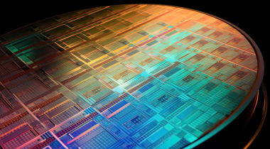
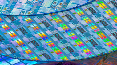
AI GeneratedThe eBeam Initiative's annual lunch at SPIE Advanced Lithography and Patterning highlighted progress in curvilinear masks, EUV adoption, data handling, and multi-beam mask writers. Aki Fujimura discussed the feasibility and benefits of entirely curvilinear masks enabled by GPU computing and multi-beam writing. Tekscend Photomask's COO, Mike Hadsell, emphasized the importance of curvilinear masks in extending ArF equipment life and their role in lithography advancements. imec's Yi-Pei Tsai presented on managing curvilinear data size for mask-to-wafer fidelity. The eBeam Initiative aims to capture industry perspectives on trends and challenges through its Luminaries survey.