Breakthrough Thin GaN Chiplet Technology
Source
Published
TL;DR
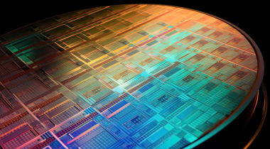
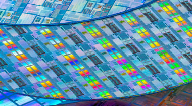
AI GeneratedResearchers at Intel Foundry have developed a breakthrough thin GaN chiplet technology that combines GaN transistors with silicon-based digital circuits to enable complex computing functions directly in power chiplets. This innovation, presented at the 2025 IEEE International Electron Devices Meeting, addresses the challenge of delivering more power, speed, and efficiency in a compact space. The ultra-thin GaN chiplet, with a base silicon measuring just 19 μm thick, incorporates the industry's first fully monolithic on-die digital control circuits. This technology offers concrete improvements in data centers, wireless infrastructure, and other industries by enabling faster switching, lower energy loss, and efficient power conversion. The use of GaN material allows for higher power density, better performance at high frequencies, and compatibility with existing silicon manufacturing infrastructure.