Technology
Wonky Graphene Could Sharpen Proton Therapy
Source
IEEE Spectrum
Published
Source
Published
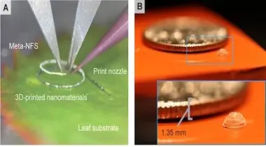
Researchers at Rice University have developed a new 3D printing process using microwaves, called Meta-NFS, that can heat nanoparticle ink with extreme precision. This technology allows for the fusing of circuits inside 3D printed objects, a capability previously unattainable with traditional manufacturing methods. Meta-NFS enables the use of a wider range of materials and improves production efficiency by adjusting microwave power in real-time. The applications of this technology include integrating electronics into soft materials like robots, implants, and plants, showcasing its potential for groundbreaking advancements in electronic manufacturing.

A chip has been developed that can project video on a scale as small as a grain of sand. Originally designed for steering lasers in quantum computers, this MEMS array technology has found new applications in image projection. Researchers have demonstrated its capabilities by projecting the Mona Lisa using a long split-electrode device. This innovation could have implications for various fields, including semiconductors, biomedical imaging, and consumer electronics.
Researchers from various universities have made significant advancements in memristor technology. At Loughborough University, a memristor reservoir computing chip was developed, showing improved energy efficiency compared to software-based solutions. At the University of Michigan, a memristor made from 2D bismuth selenide demonstrated long-term data retention and analog tuning capabilities. Additionally, researchers from the University of Cambridge, Beijing Institute of Technology, and Lund University created a highly stable, low-energy hafnium oxide memristor. These developments pave the way for more efficient and versatile AI applications in the future.

Norwegian start-up Lace Lithography, backed by Microsoft, secured $40 million in funding to develop a chipmaking tool using a helium atom beam for atomic resolution printing on silicon wafers. The technology boasts a beam width of 0.1 nanometers, significantly narrower than ASML's EUV scanners. Lace's system, named "BEUV," surpasses traditional lithography by utilizing neutral helium atoms instead of photons, potentially enabling chip manufacturers to achieve "ultimately atomic resolution." While Lace's innovative approach differs from other lithography alternatives, transitioning from prototype to production remains a significant challenge, with a target for a pilot fab test tool by 2029.
We use cookies to ensure you get the best experience on our website. For more information on how we use cookies, please see our cookie policy.