Back to home
Technology

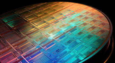
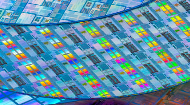
Impact Of The Film Transfer And Grain Size On The Cu-barrier Properties Of 2D WS2 Films (NUS et al.)

Source

SemiEngineering

Published

TL;DR

AI Generated

Researchers from the National University of Singapore, AIXTRON, IMiF, and Applied Materials published a technical paper on enhancing the Cu-barrier properties of 2D-WS2 barriers. They explored the role of grain size and surface passivation in maximizing the efficiency of 2D films for back-end-of-line metal interconnects. The study focused on large grain WS2 films and demonstrated that hydrogen disulfide passivation can help overcome film transfer challenges. Results showed that large grain size 2D films exhibit enhanced barrier efficiency compared to commercially available TaN systems, proving their advantage in reducing metal diffusion in BEOL dielectrics.

Read Full Article

Similar Articles

Scientists solve decades-old 2D physics puzzle — Chaotic growth in a 2D quantum system obeys statistical laws

Scientists solve decades-old 2D physics puzzle — Chaotic growth in a 2D quantum system obeys statistical laws

Researchers at the University of Würzburg have confirmed a 40-year-old physics theory by demonstrating that chaotic growth in a 2D quantum system follows the Kardar–Parisi–Zhang (KPZ) equation. This breakthrough, published in Science, extends the KPZ model to more realistic 2D environments, improving understanding of complex growth processes in non-equilibrium systems. By engineering a controlled quantum system using a GaAs semiconductor cooled to near absolute zero, the team generated polaritons to study growth dynamics. Through spectroscopy and interferometry, they observed that the behavior of polaritons aligns with statistical patterns predicted by the KPZ equation in two dimensions.

Tom's Hardware
Researchers find a way to heat 3D printer filament using microwaves, enabling fusing circuits inside printed objects — tech supports precise heating down to the width of a human hair

Researchers find a way to heat 3D printer filament using microwaves, enabling fusing circuits inside printed objects — tech supports precise heating down to the width of a human hair

Researchers at Rice University have developed a new 3D printing process using microwaves, called Meta-NFS, that can heat nanoparticle ink with extreme precision. This technology allows for the fusing of circuits inside 3D printed objects, a capability previously unattainable with traditional manufacturing methods. Meta-NFS enables the use of a wider range of materials and improves production efficiency by adjusting microwave power in real-time. The applications of this technology include integrating electronics into soft materials like robots, implants, and plants, showcasing its potential for groundbreaking advancements in electronic manufacturing.

Tom's Hardware
SemiEngineering

Silicon Photonics Lights The Way To More Efficient Data Centers

Silicon photonics is paving the way for more efficient data centers by potentially increasing bandwidth density and reducing power consumption, particularly driven by AI workloads. However, challenges such as process compatibility, thermal issues, and mechanical stress arise due to the use of various materials in photonic interconnects. Integrated electro-optical I/O modules are the desired outcome, but design and process complexities need to be addressed. The article delves into the technical aspects of silicon photonics, including the components involved, such as light sources, modulators, waveguides, and photodetectors, as well as the challenges of integrating optical and electronic components for efficient data transmission.

SemiEngineering
Chip Can Project Video the Size of a Grain of Sand

Chip Can Project Video the Size of a Grain of Sand

A chip has been developed that can project video on a scale as small as a grain of sand. Originally designed for steering lasers in quantum computers, this MEMS array technology has found new applications in image projection. Researchers have demonstrated its capabilities by projecting the Mona Lisa using a long split-electrode device. This innovation could have implications for various fields, including semiconductors, biomedical imaging, and consumer electronics.

IEEE Spectrum

We use cookies

We use cookies to ensure you get the best experience on our website. For more information on how we use cookies, please see our cookie policy.